The development of an ability to "see at night" has been the subject
of research and development for
many decades. Night vision is usually achieved by using staring infrared
focal plane detector arrays.
Infrared focal plane arrays have both commercial and defense applications.
Some examples of
commercial applications include: visual aids for automobile drivers
so that they can see beyond
oncoming headlight glare and well beyond the normal range of the vehicle
headlights; visual aids for
commercial aviation for use in conditions of reduced visibility; monitoring
industrial machines and
processes for proper operation temperature with non-contact IR-imaging;
and thermal imaging in
medicine (thomography). Security, fire and search and rescue services
will benefit from the
availability of low cost night vision infrared imagers. Defense applications
include: night vision, low
visibility target detection, tracking and remote earth observations.
Most infrared detectors have centered on the 3-5 mm (MWIR) and the 8-12
mm (LWIR)
wavelength bands because of the high atmospheric transmission at these
wavelengths. Detection in
the 3-5 mm range has been traditionally achieved by InSb based detectors
while the 8-12 mm range
has been covered by detectors made of HgCdTe. On the other hand, recent
emerging technologies
such as quantum well based detectors and uncooled thermal sensors using
silicon microbolometers
provide many advantages over conventional detectors. These include
the capability of multicolour
detection for identification of objects and more importantly uncooled
detectors for low cost thermal
imaging. In this article, we report some of the recent work that has
being carried out on multicolour
detectors and silicon based uncooled microbolometers.
Bolometer infrared sensors operate by converting the incident infrared
radiation into a temperature
rise of its supporting membrane. This temperature rise causes the resistance
of a resistive sensing
element attached to the membrane, to change by an amount proportional
to the incident infrared
power. To increase the sensitivity of detection, it is necessary to
miniaturize the bolometer and
improve its isolation from the substrate. This is usually done by silicon
micromachining which reduces
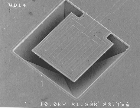
the thermal conductance between the sensor and the substrate. Figure
1 shows a silicon
microbolometer fabricated using micromachining. This work was performed
in collaboration with the
Institute of Microelectronics (IME). Since the heat capacitance of
the bolometer is relatively small, it
can experience a significant temperature rise under a weak infrared
power (10 nW). By monitoring
the resistance change of the sensor, the corresponding infrared signal
can be detected. This is usually
achieved by passing a bias current through the sensor element and measuring
the resultant voltage
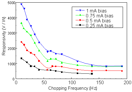
drop across the sensor element. Figure 2 shows the measured infrared
response of a
microbolometer at room temperature. The roll-off of the frequency response
of the sensor gives the
limit of operating speed which is determined by the thermal time constant.
Another area of interest is the fabrication of multicolour detectors
to enhance the performance of
detection, in particular, for discrimination of objects and imaging
under varying atmospheric
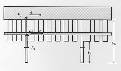
conditions. To obtain a response at two wavelengths, an InGaAs/GaAs
step quantum well designed
to have three energy levels (E1, E2 and E3) as illustrated in Figure
3, was employed. The asymmetry
of the step quantum well distributes the oscillator strength between
the two transitions, E1 ® E2 and
E1 ® E3. The E1 and E2 states are bound and are located in the
step quantum well while the E3 is
positioned just above the barrier to efficiently collect the photoexcited
carriers. However, the E2
level is much lower than the barrier height which makes its harder
for the E1 ® E2 photoexcited
electrons to escape from the quantum wells. To overcome this difficulty,
we employed a 5-period
AlGaAs/GaAs superlattice barrier, with the first miniband aligned with
the E2 state in the quantum
well, as schematically shown in the Figure 3. This allows the photoexcited
electrons to move along
the miniband.
The QW multicolour detector structure used in this study was grown on
a semi-insulating (100)
GaAs substrate by molecular beam epitaxy (MBE). It has 20 periods of
step quantum wells and
superlattice barriers sandwiched between two 1 mm thick GaAs layers
doped with Si to 1´ 1018
/cm3 for ohmic contacts. The step quantum well consists of a 30 Å
thick In0.3Ga0.7As well doped
with Si to 1´ 1018 /cm3 and a 73 Å thick undoped GaAs step.
The thickness of the InGaAs layer in
the step quantum well was kept below the critical thickness corresponding
to the 30% in
composition. The superlattice barrier that separates the step quantum
wells consists of undoped
5-periods of 51 Å thick GaAs wells and 40 Å thick Al0.26Ga0.74As
barriers. For the infrared
response measurement, diodes of 200 mm ´ 200 mm were fabricated
using standard
microelectronics processing techniques.
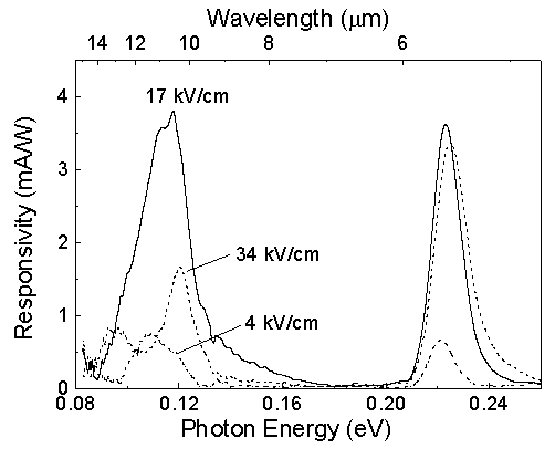
The spectral dependence of the photoresponse was measured using a ceramic
infrared source
coupled to an Oriel MS257 grating monochromator with lock-in detection.
Figure 4 shows the
responsivity (mA/W) as a function of the incident photon energy for
several bias voltages at 60 K.
The photon flux as a function of wavelength was measured simultaneously
using a calibrated
pyroelectric detector. There are two peaks of the photoresponse at
about 110 meV and 220 meV
corresponding to the E1 ® E2 and E1 ® E3 transitions, respectively.
Source: Engineering Research News, National University of Singapore,
Feburary 1998