Gallium Nitride (GaN) is a semiconductor that has received attention
lately because of its wide
band-gap. Wide band-gap materials are necessary for the realisation
of semiconductors that emit in
the blue to ultra-violet regions of the spectrum. The significance
of blue and ultra-violet emission is
due to its shorter wavelength resulting in less diffraction compared
with infrared emission, and hence
allows higher optical recording densities on CD-ROMs, and higher resolution
of laser printers. Like
other semiconductor materials, their successful application requires
accurate knowledge of their
electronic properties. This article describes the results of some recent
investigations of GaN based
materials carried out at COE.
The intrinsic and extrinsic properties of GaN based semiconductors have
been systematically
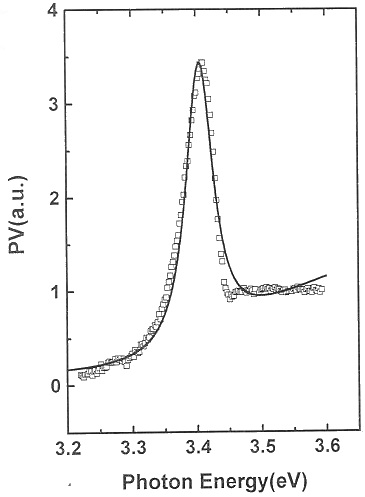
investigated by optical and electrical methods. A clear exciton absorption
peak as shown in Figure 1
has been observed for the first time at room temperature by photovoltaic
(PV) spectra, for a GaN
layer grown on (0001)-plane Sapphire by metalorganic chemical vapour
deposition. From the
spectra, the Wurtzite GaN room temperature A and B exciton transition
energies and the energy gap
have been obtained, and are 3.401 eV, 3.408 eV and 3.426 eV respectively.
We have also
performed photovoltaic measurements with varied light incidence angle,
and observed the
polarisation behaviour of exciton absorption in GaN. Phonon-assisted
photoluminescence (PL) in an
Wurtzite GaN epilayer was also measured at different temperatures.
Besides the exciton emissions,
longitudinal optical (LO) phonon-assisted PL associated with both bound
exciton and the free
exciton were observed. The study of the 2LO phonon replica can provide
information of the
temperature dependence of the concentration and recombination lifetime
of free excitons in GaN.
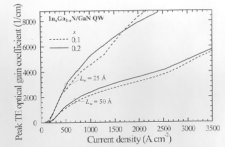
We have also systematically investigated the electronic band structures
of Zinc-Blende and Wurtzite
GaN based bulk and Quantum Well (QW) semiconductors by pseudopotential
and k.p methods.
For the Zinc-Blende QW structures, the energy bands are sensitive to
the strain due to the lattice
mismatch between the substrates and different layers. Consequently,
the compressive strain
enhances the TE mode optical gain and strongly depresses the TM mode
optical gain. The laser
threshold current density is 0.53 kA/cm2 for the 100Å well width
GaN/Ga0.85Al0.15N QW
structure. For the Wurtzite QW structure, the energy bands are not
as sensitive to the strain due to
the symmetry property of the Wurtzite crystals. The effect of Al mole
fraction and the well width to
the Laser action has been investigated to optimise the Laser Diode
design (see Figure 2).
Source: Engineering Research News, National University of Singapore, Feburary 1998